EMBEDDED SYSTEMS PROJECTS (ARM/FPGA)
This page contains the details of a personal project (LPC1114) and projects I completed as part of my coursework.
LPC1114 (ARM M0)
My main goal for this project was to program and add hardware components to an ARM chip from as basic a level as possible, while still utilizing the main development tools (JTAG debugger, CMSIS etc) . I find using development boards obscures the underlying hardware and software development, making it more difficult to understand the underlying principals. The LPC1114 chip was chosen for its relatively simple processor (M0) and the DIP package. This chip package allows for breadboard prototyping. The only other DIP ARM chip is the LPC810 (M0+), which also is capable of single wire debugging (SWD), but has limited pins. Here I outline the setup that I use to start projects.

Below is the schematic interfacing the JTAG debugger with the LPC1114. The 5V signal has to be stepped down to somewhere between 1.8 and 3.6V for the microcontroller (I used 3.3V using a MCP1700).


Adafruit makes two great adapters (JTAG to SWD) and the SWD breakout board. Unfortunately, there is no 5V pin on the SWD breakout board, but there is a 5V pin on JTAG. In order to use this pin I just soldered to the pad. If using Segger J-Link, the 5V pin may have to be activated using the 'j-tag commander,' part of the J-link software.

I have used some open-source programmers with little luck and a huge amount of frustration. I have had the most success with the Segger J-Link, it is ~$64 on Digi-Key. I use the code size limited IAR Embedded Workbench. Both these tools make development extremely simple and straightforward. Ideally, You should be able to download the header files from the manufacturer (LPC), but they are unfortunately not on their website. The LPC1114 header files were found by downloading Keil MDK-Lite from ARM. Within the software (Project => Manage => Pack Installer) and find the chip.

GROUP CLASS PROJECTS
COMPUTER DESIGN (FPGA based)
The overall goal of the class was to design a 16 bit RISC processor on a Spartan 6 FPGA (architecture and instruction set) that ran a hardware project.

My lab partner and I designed a system that wirelessly controls various functions on an aquarium. The main user interface was through a touchscreen which displayed buttons. Each of these buttons corresponded to change in a peripheral state.
The overall system can be divided into three parts: the touchscreen interface, wireless communication and peripheral control. Each of these segments required specialized hardware and software development, whether on the FPGA or arduinos. The touchscreen interface required the development of specialized CPU instructions, hardware design and software. Instructions were created to control both the timing of the CPU, as well as interface with user input on the touchscreen.


The touchscreen can be divided into three parts: the development of glyphs and their storage and access in memory, the display of the glyphs and the touchscreen sensor.
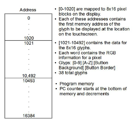
Our overall memory management is illustrated in the following figure (left). The first elements of memory are the glyphs, the locations of the beginning of the glyphs, the next area contains memory elements that map to regions of the display (entering the memory location of a glyph at these addresses will cause them to be displayed), then the program memory. The timing schematic for the touch screen sensor (right) illustrates the challenges of updating the screen. Another challenge was getting the X and Y location of the touch sensor data.

The overall system is illustrated in the figure below. The touch screen initially displays 4 buttons, heater and bubbler both set to OFF. The user touches a button and the screen updates with their selection. In the case illustrated in the figure, the user chooses the ‘LIGHTS’ button. The second pane showing the light options is then displayed. Once a light selection is made, the code for that peripheral state is sent to the arduino master and subsequently sent over the NRF24L01 wireless module. After sending the 8 bit code to the Arduino, the original pane is displayed and updated with the current state of the peripherals.

EMBEDDED SYSTEM DESIGN (ARM M3)